11.1 PURE RESISTANCE, INDUCTANCE OR CAPACITANCE
It is shown in Chapters 8, 9 and 10
that opposition to the flow of current when an alternating voltage is applied
to a circuit can be caused by any one or more of the following:
·
resistance
(R)
·
inductive
reactance (XL)
·
capacitive
reactance (XC)
All are measured in ohms, and,
provided that only one of the three is present at any one time - that is, that
the resistance or reactance is ‘pure’ - the current which flows is governed by
Ohm’s Law, namely:

where V and I are rms values.
In this chapter will be considered
how the current is affected if more than one of these factors are present.
11.2 RESISTANCE PLUS INDUCTIVE REACTANCE
Suppose that there is a series
circuit containing a resistance R and
an inductance L. If the frequency f is known, the inductive reactance XL = 2pfL, so XL also is
known.

FIGURE 11.1
RESISTIVE/INDUCTIVE
CIRCUIT
If the pair of elements R and XL are fed in series from an a.c. supply voltage V, they will have a common current I.
This is shown as the red vector I
in Figure 11 1.
Since current I passes through the pure resistance R, it will be in phase with the voltage IR developed across it, the magnitude of this voltage being
determined by Ohm’s Law V = IR. This is shown as voltage vector IR (full line) in Figure 11.1, where it
is in phase with the current I.
The same current I also passes through the pure inductive
reactance XL. The current I through XL
will lag 90° on the voltage IXL
across it, the magnitude of this voltage being determined by Ohm’s Law V = IXL
for a pure inductance. As the current I lags 90° on voltage IXL,
voltage IXL leads
on the current I and is shown as
voltage vector IXL (full
line) in Figure 11.1.
Thus the total
voltage across R and XL is the vector sum
of IR and IXL, which has been shown in Chapter 7 as being the
diagonal of the rectangle formed by IR
and IXL - that is, the
line OP. It can be written:

This combined
voltage is of course the same as the applied voltage V, so that:
V = I
(R + XL)

This shows that, for a combined
resistive/inductive circuit, Ohm’s Law applies if the vector sum of R and XL is substituted for R. This vector sum is called
the ‘impedance’ of the circuit; it has the symbol ‘Z’ and is measured in ohms.
Numerically) from the right-angled
triangle formed by the diagonal OP and the vectors IR and IXL,

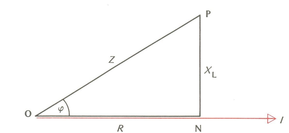
FIGURE 11.2
IMPEDANCE TRIANGLE
This triangle OPN is called the
‘impedance triangle’ (Figure 11.2) of the circuit and enables the impedance to
be calculated, or measured directly, if R
and XL are both known.
11.3 RESISTANCE PLUS CAPACITIVE REACTANCE
Suppose that there is a series
circuit containing a resistance R and
a capacitance C. If the frequency f is known, the capacitive reactance  , so XC
also is known.
, so XC
also is known.
, so XC
also is known.
FIGURE 11.3
RESISTIVE/CAPACITIVE
CIRCUIT
If the pair of elements R and XC are fed in series from an a.c. supply voltage V, they will have a common current I.
This is shown as the red vector I
in Figure 11.3.
 . The impedance
triangle OPN is similar but inverted.
. The impedance
triangle OPN is similar but inverted.
Ohm’s Law for a resistive/capacitive
circuit is, as for the resistive/inductive case,  ohms, where
  .
.
ohms, where .11.4 GENERAL CASE - OHM’S LAW FOR A.C.
For a circuit containing resistance
and reactance, whether inductive or capacitive reactance, or both, Ohm’s Law
applies in the form:

The reactance X is, in the general case, the sum of all reactances in the
circuit, whether inductive or capacitive, remembering that capacitive
reactances are regarded as negative.
In the special case where the
inductive and capacitive reactances are numerically equal (but opposite), XL = -XC, or XL
+ XC = 0.
In that case the expression (ii) for Z
reduces to:

Z has then its minimum value and behaves
as a simple resistance. With Z at a minimum, equation (i) shows that I is at its maximum - we have a
condition known as ‘resonance’.
11.5 PHASE ANGLE
In Figure 11.2 the angle between OP
and ON (the Z and R vectors) is called the ‘phase angle’
and is given the Greek symbol ‘j’ (phi, for ‘phase’). From the trigonometry of the impedance
triangle:

so that, if any two of R, X
and Z are known, the phase angle j can be determined. Also, if X is capacitive (= XC), it is by convention negative, so that j too is negative and below the line.
If j above the line represents a lagging phase angle, below the line it
represents a leading phase angle.

FIGURE 11.4
IMPEDANCE - GENERAL CASE
In the special cases (a) where there
is only resistance and no reactance, X
= 0 and therefore  = 0; (b) where there is only reactance and no resistance, R = 0 and therefore
= 0; (b) where there is only reactance and no resistance, R = 0 and therefore = 90°. That is to say, in these
two special cases of pure resistance and pure reactance the phase angles are 0° and 90° (lagging or leading) respectively, which are precisely the situations
shown in Figures 8.1, 9.2 and 10.2 respectively, where the current is in phase
or 90° lagging, or 90° leading, on the voltage.
In the general case where there is
both resistance and reactance, the phase angle lies somewhere between 0° and +90° for inductive circuits, and between 0° and -90° for capacitive circuits.
Figure 11.4 shows the two general
cases of a partly inductive and a partly capacitive circuit, where it will be
seen that the current lags, or leads, on the voltage by an angle which is less
than 90° and which is, in fact, the phase angle .
.
No comments:
Post a Comment